Visualizing Fine Scratches on Mirror-Like Surfaces | TR-300 Clearly Captures Polishing Marks on a 6-Inch Silicon Wafer
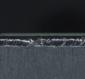
A mirror-like polished surface looks beautiful to the eye. However, in the world of visual inspection, this “mirror surface” is one of the most challenging targets. Because a mirror-like surface reflects illumination directly, the camera captures the light source itself, and the fine scratches on the surface are buried in the reflected light.
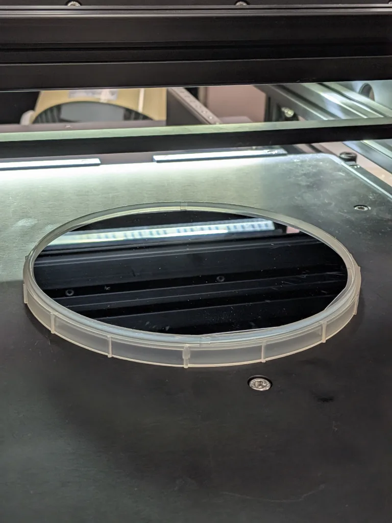
TOMOMI RESEARCH Inc. has successfully demonstrated, using its AI visual inspection system “TR-300,” that fine defects such as polishing marks and scratches on the mirror surface of a 6-inch silicon wafer can be clearly visualized without being affected by specular reflection from the illumination. This was an internal technical demonstration.
Why Is Mirror Surface Inspection So Difficult?
ost visual inspection methods shine light onto the target object and capture the reflected light, or brightness, with a camera to detect defects. The basic idea is simple: if there are surface irregularities or scratches, the reflection of light is disturbed, and those defects appear as brightness variations in the image.
However, a mirror-like surface causes “specular reflection,” meaning that the incoming light is reflected almost entirely in a single direction. As a result, what enters the camera is the image of the light source itself. Most of the captured image either becomes almost completely dark or shows the illumination as a bright reflection. Fine polishing marks and scratches on the surface are swallowed by the intense reflected light.
In other words, with mirror surfaces, the conventional assumption of detecting defects as differences in brightness no longer works. Capturing fine scratches on a mirror-like surface without being affected by reflected illumination has traditionally been considered extremely difficult.
Before and After: Fine Scratches Emerging from a Dark Mirror Surface
First, please take a look at the demonstration results in the images.
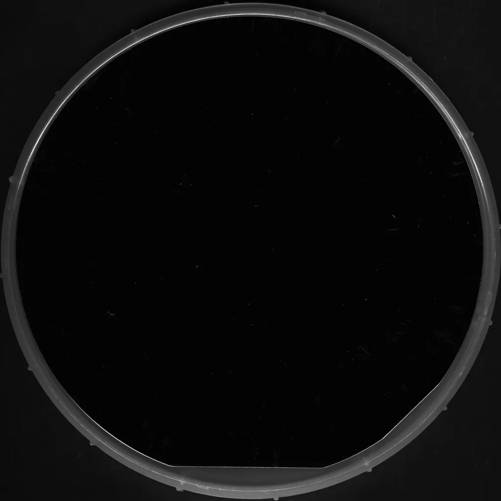
In the before image (normal imaging), the mirror surface of the 6-inch wafer appears almost completely black. Even when looking carefully, only very faint scratch lines can barely be seen, making it extremely difficult to evaluate the surface condition.
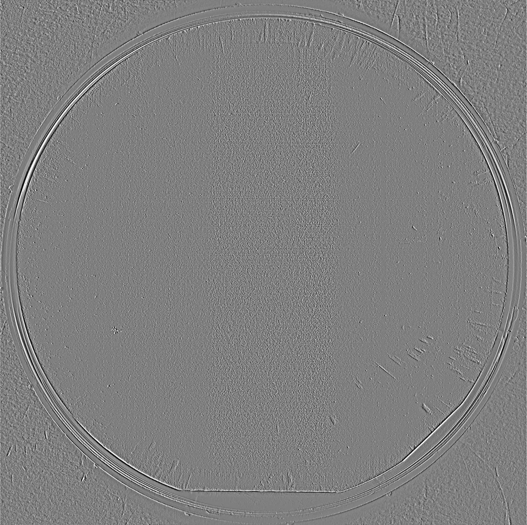
In the after image (TR-300 processing result), concentric, arc-shaped polishing marks and scratches clearly emerge on a uniform gray surface with a three-dimensional appearance. Fine defects that could not be captured by the naked eye or a standard camera have now become clearly visible.
How Was This Possible? Seeing “Shape” Instead of “Brightness”
The key point is that TR-300 does not rely on “brightness” alone.
TR-300 is equipped with TOMOMI RESEARCH’s proprietary 3D imaging technology, FORESIGHT STEREO®, which is an advanced development of photometric stereo. The system captures images while controlling illumination from multiple directions, then uses that information to acquire 3D surface irregularities.
This is the important point. Even if the entire surface strongly reflects illumination like a mirror, the surface orientation at the exact point of a scratch is slightly different from the surrounding area due to tiny irregularities. Because TR-300 uses shape information, not brightness, as the key signal, it can extract the “shape” of fine defects hidden beneath reflected illumination.
The acquired 3D surface information is then analyzed by our AI anomaly detection software, E3 ENGINE®, which identifies abnormal areas. In other words, polishing marks and scratches that emerge as shape information are detected by AI as defects. This combination — “capturing shape with FORESIGHT STEREO® and identifying anomalies with E3 ENGINE®” — provides a breakthrough approach to the difficult challenge of mirror surface inspection.
What Is TR-300? Inspecting Every Part on a Moving Production Line
This mirror-surface wafer demonstration is a natural extension of TR-300’s core strengths.
3D acquisition of surface irregularities:
TR-300 can detect subtle defects that are difficult to identify with 2D flat images, such as fine scratches hidden in colors or patterns, and dents on glossy surfaces.
Imaging, 3D reconstruction, and AI judgment completed in approximately 34 ms*:
Thanks to its high-speed processing, TR-300 enables 100% inspection on continuous conveyor lines. The ability to continuously perform 3D imaging inspection on moving production lines is a key technical breakthrough.
*Processing speed and “among the fastest in the industry” are based on TOMOMI RESEARCH’s internal evaluation.
Support for wide and long products:
By combining line-scan cameras with proprietary illumination control, TR-300 supports 4K, 8K, and 16K configurations. It can be applied to wide and long products such as steel plates, films, and long metal components.
TR-300 has been developed for 100% inspection of a wide range of products, including automotive parts, steel plates, metal sheets, films, electronic and precision components, cosmetic containers, and pharmaceutical packaging. In particular, it has demonstrated strong performance in inspecting glossy products such as bearings, plated parts, and curved metal components.今回の鏡面ウェハの事例は、TR-300がもともと持つ強みの延長線上にあります。
The First Step into a New Field: Semiconductor Silicon Wafers
This strength, developed through the inspection of glossy products, has now shown the potential to be applied to an even more challenging target: the mirror surface of semiconductor silicon wafers.
Quality assurance in semiconductor and wafer manufacturing is an area where requirements become increasingly strict as devices continue to become smaller and more highly integrated. The fact that TR-300 was able to capture fine scratches on a mirror-like surface without being affected by illumination reflection confirms one possible path into this new field.
That said, this is still an internal technical demonstration. We do not intend to claim that TR-300 can solve all challenges in semiconductor inspection. Rather, this result should be regarded as a first step in confirming its applicability to a new and extremely difficult inspection target. We will continue to carefully validate its value while listening closely to feedback from actual manufacturing sites.
Conclusion
In response to the conventional belief that “scratches on mirror surfaces cannot be captured,” TR-300 offers one possible answer: seeing shape instead of brightness. We hope this article provides a useful introduction to a new inspection approach for those facing challenges with mirror-like or glossy surfaces, as well as those involved in quality assurance for semiconductor and wafer manufacturing.
Are you struggling to inspect difficult targets such as mirror surfaces, glossy surfaces, or silicon wafers?
We offer technical consultations and demonstrations using TR-300. We also welcome inquiries such as, “Can this specific object from our production site be inspected?”
Please feel free to contact us through the inquiry form on the official TOMOMI RESEARCH Inc. website, or by phone or email.
Official website: https://www.tomomi-research.com/
Contact: info@tomomi-research.com / Tel: 0466-54-9003