What If One Capture of a Semiconductor Chip Let You See "Color" and "Shape" Separately? Observing a Semiconductor Surface with TR-100
 kotai2003
A semiconductor chip surface is one of the most "distracting" subjects in visual inspection. Thin-film interference colors sit on top of a metallic luster, and purple, green, red, blue, and yellow mix together like a soap bubble. That vividness completely buries the "shape" you actually need to see. Is it a step in the wiring, or just color unevenness? A fine relief, or dirt sitting on the surface? To the human eye or an ordinary camera, "color" and "shape" melt together in a single image and cannot be separated.
So what if you could extract "color" and "shape" as separate layers from just one capture of the same chip? In this post, we captured a semiconductor chip with our AI visual inspection system TR-100 and present the results of generating four outputs simultaneously from a single capture using its built-in technology, FORESIGHT STEREO®. Peel away the vivid colors and let only the shape rise to the surface. Follow the process with actual images.
*This article is a demo observing a single sample and does not guarantee general detection or measurement performance.
Starting with the subject: a copper-colored chip a few centimeters square
First, let us look at the subject.
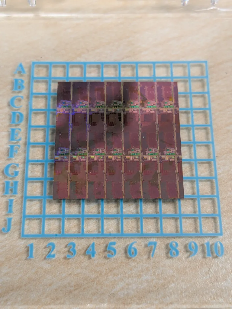
The semiconductor sample on a blue grid mat. Compared with one grid square, it is roughly a few centimeters square.
On the blue grid cutting mat sits a square sample a few centimeters across, with a copper to reddish-purple metallic luster. On its surface, regions divided like vertical stripes are neatly arranged. This is a grid layout for building many copies of the same circuit on silicon and later cutting them apart (dicing). Each section is called a die, and the grooves that separate the dies are called scribe lines (dicing streets).
That is as far as the naked eye can go. What fine patterns, with what relief, are built into each die? Beyond this point, it is TR-100's turn.
TR-100 and FORESIGHT STEREO®: how four images are extracted from one capture
TR-100 is our AI visual inspection system (product). It is the TR-100 that we used for this capture, and at its core is our 3D imaging technology, FORESIGHT STEREO®.
FORESIGHT STEREO® is our own development of Photometric Stereo, a method that combines images captured with light from multiple directions, calculates the surface slope (normal) point by point, and builds up the shape. Think of how the shadow of a slight step on a dark floor changes depending on whether you shine a flashlight from the left or the right, and imagine doing that with industrial precision.
With this mechanism, TR-100 generates the following four outputs simultaneously from a single capture.
- LIVE image: full color as seen (color and shape mixed together)
- 2D Texture: a "color only" image with shading removed
- 3D Surface: a "shape only" image with color removed
- Surface Normal: an intermediate representation of the 3D reconstruction that expresses surface orientation as color
The key point is that these are not separate recaptures but four ways of seeing taken from the same single capture. Now let us go through them one at a time, in the order "color, then shape."
Output 1: LIVE image, the as-seen state with color and shape mixed
This is the LIVE image captured by TR-100.
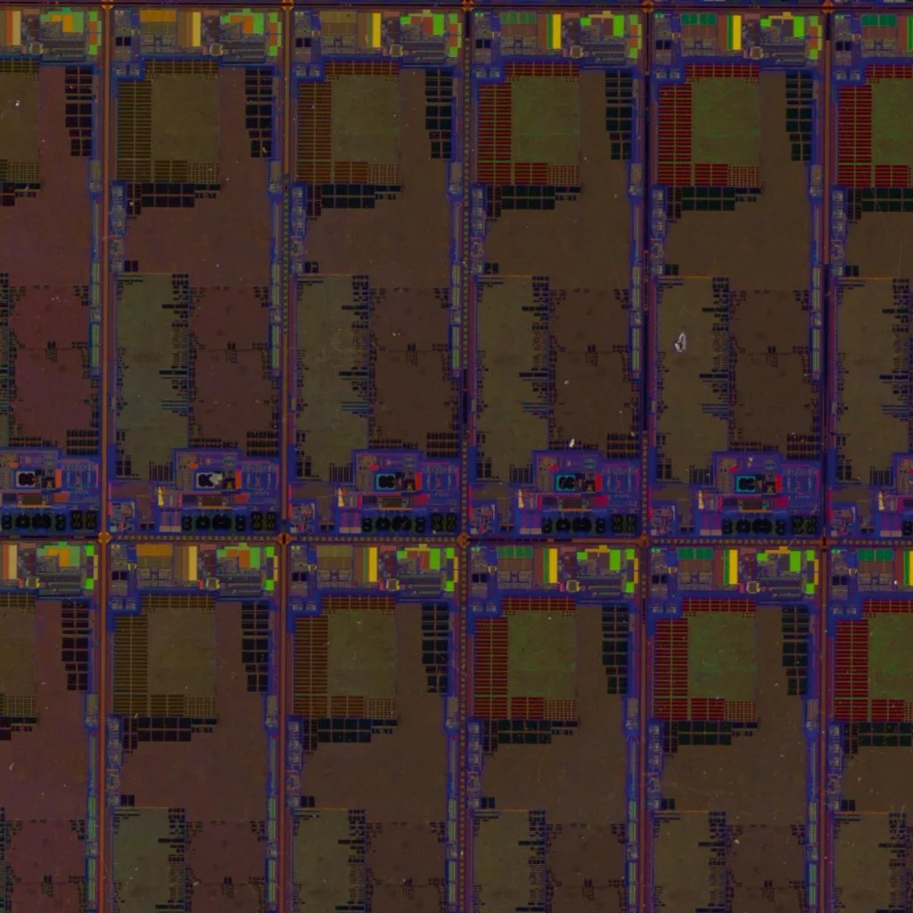
LIVE image. Thin-film interference colors overlay the image, and the grid of dies and the fine circuit patterns inside them appear vivid.
The dies arranged in a grid, and the fine patterns of wiring and blocks built into them, are colored in vivid purple, green, red, blue, and yellow. Most of this color is interference color produced when a thin film on the surface makes light interfere. It works on the same principle as the rainbow colors of a soap bubble or an oil film; it is not painted-on color but color seen through light interference.
Look closely, and you can also see a bright, point-like spot toward the right of the image that differs from its surroundings. Is this color unevenness, or something sitting on the surface? In this state, "color" and "shape" are melted into one image, and you cannot tell. This is the starting point for visual inspection of semiconductor surfaces.
Output 2: 2D Texture, removing shading to extract "color only"
Next is the 2D Texture, taken from the same capture.
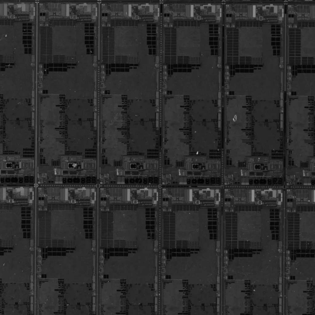
2D Texture. An image that removes shading (the cue for relief) and keeps only the color and pattern of the material itself.
Here, shading (the cue for three-dimensional form) is removed and only the albedo, the color and reflectance of the material itself, is extracted. It is like erasing the shading from a coloring page and keeping only "the color of the paint."
The patterns are now flat and readable at a uniform brightness. The vivid interference colors from before have settled down, and "which pattern (texture) sits where" can be seen plainly. In other words, this is an image that deliberately discards the cues for shape and keeps purely the "color information." Next, let us do the opposite.
Output 3: 3D Surface, remove the color and the "shape" rises (the highlight of this article)
The image we most want you to see this time is this 3D Surface.
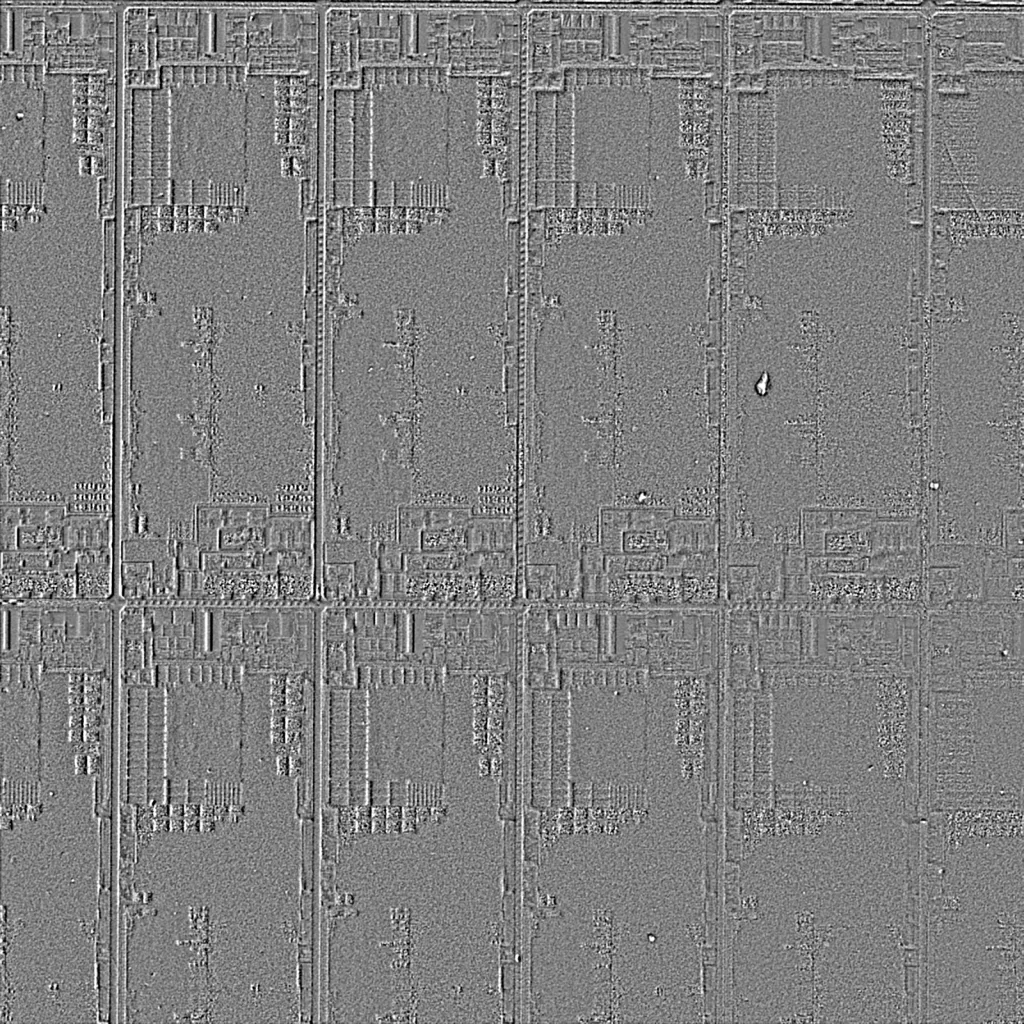
3D Surface. An image that strips away all color and brings out only the "relief (shape)," like a plaster relief.
The vivid interference colors have disappeared entirely. What has risen in their place is "physical relief" such as steps in the circuit structure, block edges, and the grooves of the scribe lines. It is as if all the color had been peeled away, leaving only a plaster relief. Even the fine undulations created by the wiring patterns inside the dies can be read as shape.
What matters here is the contrast with outputs 1 and 2. Most of the color that looked vivid in the LIVE image and the 2D Texture barely appears in the 3D Surface. In other words, it becomes clear that the vividness was "color," not "shape." Conversely, the fine relief that was hard to see under the colors finally takes center stage once the color is removed. This reversal from "color" to "shape" is the core of FORESIGHT STEREO®.
Output 4: Surface Normal, expressing the "orientation" of the surface as color
Finally, the Surface Normal.
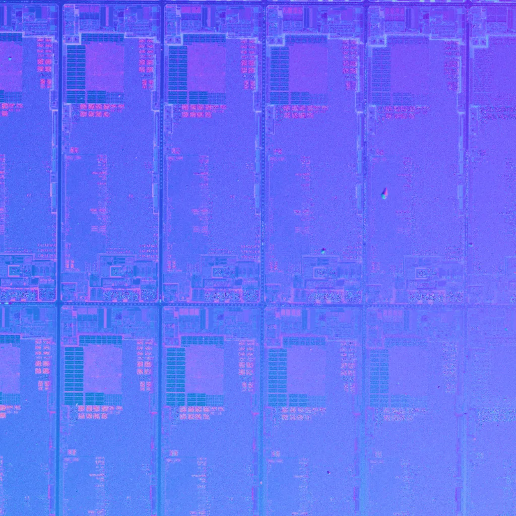
Surface Normal. An intermediate representation of the 3D reconstruction that replaces the surface orientation (normal) at each pixel with color.
The Surface Normal encodes the surface orientation (normal vector) at each pixel as color. It may help to imagine a map in which slopes are colored by the direction they face. The overall blue to purple tint indicates that most of the surface faces straight up (is flat).
At edges and pattern boundaries, changes in orientation appear as reddish accents. Note the point-like spot toward the right that we saw in the LIVE image. In the Surface Normal as well, a change in orientation (a disturbance in color) that differs from its surroundings can be seen near that spot. This is the "map of orientation" partway through building the 3D Surface, and also an image that lets you check from behind the scenes how the shape is being reconstructed.
What can you learn by comparing "color" and "shape"?
With all four outputs in hand, information that was mixed in a single image can be read by comparing them against each other.
Take the point-like spot seen in the LIVE image. If it appeared only in the 2D Texture (the color image) and not in the 3D Surface (the shape image), it could be "a stain or discoloration that is only color." Conversely, if it also appears in the 3D Surface or Surface Normal as a change in orientation or relief, the possibility of "something sitting three-dimensionally on the surface" comes into view.
In this sample, the point-like spot left cues in both the color image and the shape image, showing that there is more material for observation to distinguish "a color-only stain" from "three-dimensional foreign matter." Holding color information and shape information in separate layers adds one more level of cues for judgment.
*This is only a suggestion based on observing a single sample and does not guarantee detection performance for defects or foreign matter.
How does this help on the inspection floor?
The ability to "separate color and shape" shown here with a semiconductor chip carries directly over to the inspection of highly reflective and glossy materials.
- Fine relief buried in interference colors or glare can be visualized as "shape": steps and undulations hidden by metallic luster or rainbow colors can be captured separately from color.
- Color unevenness (texture) and shape defects can be observed separately: it becomes easier to separate, in different layers, whether something is "a color problem" or "a shape problem."
- Color and shape can be acquired at the same time in a single capture: because both kinds of information are obtained without recapturing, you gain cues for distinguishing "a color-only stain" from "three-dimensional foreign matter."
For subjects such as silicon, metal, plating, and wafers, where it has been hard to "tell color unevenness from shape defects" on highly reflective surfaces, TR-100 offers a new entry point: observing "color" and "shape" separately.
Summary
- TR-100 generates four images that separate "color" and "shape" simultaneously from a single capture. Information that would be mixed for the human eye or an ordinary camera can be extracted as separate layers (these four outputs come from the built-in technology FORESIGHT STEREO®).
- Fine relief that is hard to see under vivid interference colors or glare can be recaptured as "shape." Colors that look vivid in the LIVE image and 2D Texture almost disappear in the 3D Surface, showing that they are color and not shape, while relief such as wiring steps and scribe-line grooves stood out clearly in the color-free 3D Surface.
- It provides cues for distinguishing "a color-only stain" from "three-dimensional foreign matter." Comparing color information with shape information increases the material for observation (*a suggestion from observing a single sample, not a guarantee of general detection performance). This is a strength that carries over to visual inspection of highly reflective and glossy materials (metal, silicon, plating, wafers).
If you would like a demo or sample evaluation of surface observation of semiconductors and highly reflective materials with TR-100, or of visual inspection that separates "color" and "shape," please feel free to contact TOMOMI RESEARCH Inc.