Visualizing Fine Flaws on Mirror Surfaces: TR-300 Clearly Reveals Polishing Marks on a 6-Inch Silicon Wafer
 kotai2003
A surface polished smooth as a mirror looks beautiful. In the world of visual inspection, however, this "mirror surface" is one of the toughest subjects of all. A mirror reflects the illumination straight back, so the camera sees the light itself, and the fine surface flaws that matter are buried in the reflected light and do not show up.
TOMOMI RESEARCH Inc. has used its 3D × AI inspection system TR-300 to clearly visualize fine flaws (polishing marks and scratches) on the mirror surface of a 6-inch silicon wafer, unaffected by the specular reflection of the illumination (an in-house technical demonstration). In this article, using actual before and after images, we explain "how we saw flaws that a mirror should make impossible to capture."
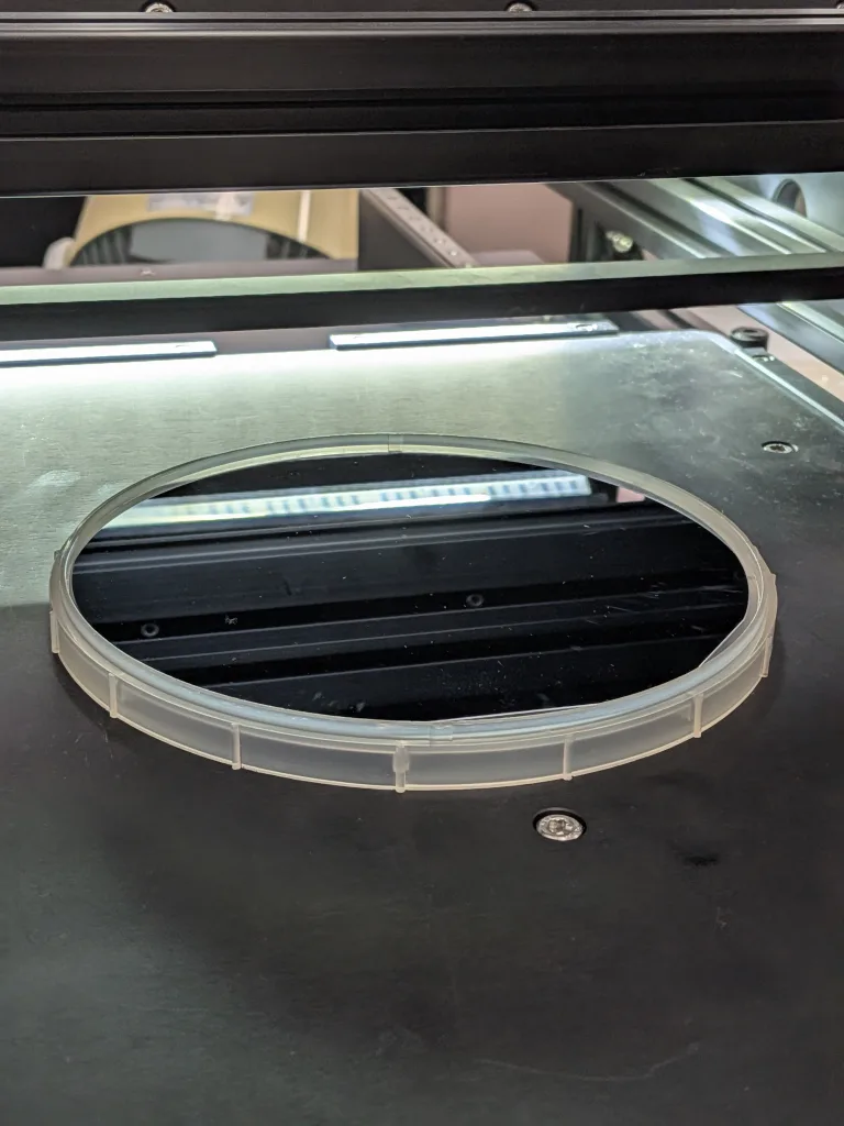
A 6-inch silicon wafer on a plastic ring on the TR-300 inspection stage, with LED light bars reflected in its mirror surface
Why is inspecting mirror surfaces so difficult?
Most visual inspection shines light on an object, captures the reflected light (that is, brightness or luminance) with a camera, and looks for flaws. Where the surface has relief or a flaw, the reflection of light is disturbed there and shows up as uneven light and dark. That is the basic idea.
A mirror surface, however, causes "specular reflection," bouncing incoming light back in one direction almost unchanged. As a result, what enters the camera is an image of the illumination itself: most of the frame either sinks to black or shows the light reflected in white. Slight polishing marks and scratches on the surface are swallowed by the intense reflected light.
In other words, on a mirror surface the conventional premise of "capturing flaws as differences in brightness" itself breaks down. Imaging fine flaws on mirror surfaces without being affected by reflections of the illumination has long been considered extremely difficult.
Before and after: flaws emerge on a pitch-black mirror surface
First, take a look at the results of this demonstration.
Before (conventional imaging): the mirror surface of the 6-inch wafer is almost pitch black. Even looking closely, you can barely make out a few very faint scuff lines, and it is almost impossible to judge the surface condition.
After (TR-300 processing result): on an even gray surface, concentric (arc-shaped) polishing marks and scratches stand out sharply in three dimensions. Fine flaws that could not be captured by the naked eye or an ordinary camera are now clearly "visible."
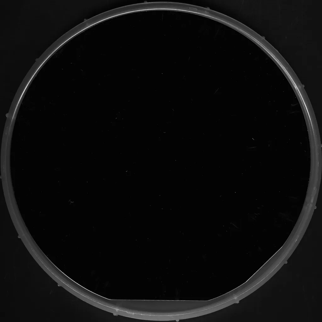
Before: with conventional imaging, the mirror surface sinks to black and surface flaws cannot be seen.
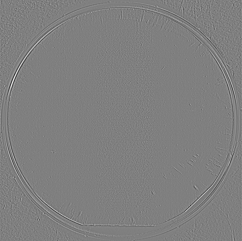
After: the TR-300 processing result. Fine polishing marks invisible to the naked eye and an ordinary camera are clearly visualized.
How was it captured? Looking at shape, not luminance
The key is that what TR-300 looks at is not "brightness".
TR-300 is equipped with our own 3D imaging technology "FORESIGHT STEREO®" (a technology we developed from Photometric Stereo). It captures images while controlling illumination from multiple directions, and from that information acquires the relief of the surface in 3D.
Here is the point. Even on a mirror surface that specularly reflects the illumination everywhere, the surface orientation (relief) at the exact spot of a flaw differs slightly from its surroundings. Because it relies on shape (relief) rather than luminance (brightness), it can pick up the "shape" of fine flaws hidden beneath the reflection, even when the illumination is reflected in the image.
On the 3D surface information obtained this way, the anomaly detection engine "E3 ENGINE®" judges the anomalous areas. The AI recognizes as flaws the polishing marks and scratches that have emerged as shape. This combination, "capture the shape with FORESIGHT STEREO® and detect the anomaly with E3 ENGINE®," was the breakthrough against the difficult subject of mirror surfaces.
What is TR-300? Inspecting every part on a moving line
This mirror-surface wafer case is an extension of strengths TR-300 already had.
- 3D acquisition of relief: Detects with high accuracy anomalies that are hard to distinguish in 2D (flat images), such as fine scratches hidden among colors and patterns, or dents on glossy surfaces.
- Capture, 3D conversion and AI judgment completed in about 34 ms*: High-speed processing makes 100% inspection possible on continuous conveyor lines. Being able to run 3D image inspection continuously on a moving line is a technical breakthrough. (*Processing speed and "among the fastest in the industry" are both based on our own research.)
- Wide and long products: With line scan cameras and our own illumination control, supports 4K/8K/16K. Can be applied to wide and long products such as steel sheets, films and long metal parts.
TR-300 has been developed for 100% inspection of a wide range of products, including automotive parts, steel sheets, metal sheets and films, electronic and precision components, and cosmetic containers and pharmaceutical packaging. It is a technology that has shown its strength particularly in inspecting "glossy products" such as bearings, plated parts and curved metal.
A first step into a new field: semiconductor silicon wafers
This time, the strength built up in inspecting glossy products has shown that it may also work on the mirror surface of semiconductor silicon wafers, an even more difficult subject.
Quality assurance in semiconductor and wafer manufacturing is a field where requirements grow stricter as miniaturization and integration advance. We regard capturing fine flaws on mirror surfaces without being affected by illumination reflections as confirming one possibility in this new field.
That said, this is still at the stage of an in-house technical demonstration. We do not claim to have solved every challenge in semiconductor inspection. This result is a "first step" that confirms applicability to a new, extremely difficult inspection subject. From here, we will carefully continue verification while listening to the voices of the field, to see what value we can deliver.
Closing
Against the common belief that "flaws on mirror surfaces cannot be captured," TR-300 has offered one answer with the idea of "looking at shape, not luminance." We hope this article helps those facing challenges in inspecting mirror and glossy surfaces, and those involved in quality assurance in semiconductor and wafer manufacturing, discover a new approach.
Struggling with hard-to-inspect objects such as mirror surfaces, glossy surfaces or silicon wafers?
We offer TR-300 demos and technical consultations. Questions such as "Can this object of ours be inspected?" are also welcome. Please feel free to contact us via the inquiry form on the TOMOMI RESEARCH Inc. official website, or by phone or email.
- Official website: https://www.tomomi-research.com/en/
- Contact: info@tomomi-research.com / Tel: +81-466-54-9003