
PCB 3D Reconstruction: Seeing Solder Pads as Shapes, Not Glare
 kotai2003
From one capture, the solder pads on a printed circuit board (PCB) appear as rows of rounded 3D mounds. In a regular photo, the same pads are little more than white glare.
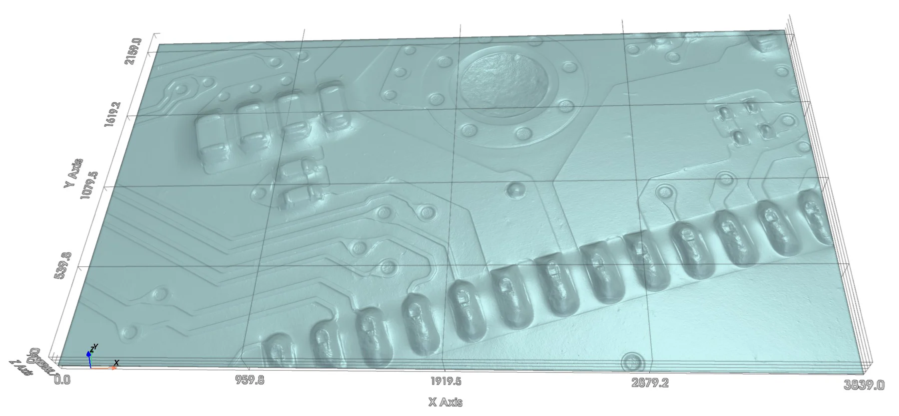
3D view in FORESIGHT STEREO Viewer. X/Y axis ticks are pixel indices, not dimensions.
We imaged the board with TR-100, using FORESIGHT STEREO® technology, and opened the result in the 3D view of FORESIGHT STEREO Viewer. In an earlier post, we compared four image outputs of another area of the same board. This time we focus on the step beyond that: 3D reconstruction.
What we imaged
- Sample: a control board from a commercial HDD, kept as an in-house sample. A good board, not a defect sample, and a different area from the earlier post.
- System: TR-100 AI visual inspection system with 8-direction lighting
- Date: November 14, 2026
- In view: green solder mask with chip components (four larger chips and two small parts), a large round hole ringed by small vias, a diagonal row of a dozen-plus elongated solder pads, and parallel traces
In a photo, solder is mostly glare
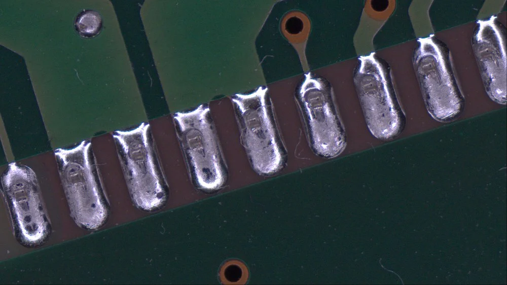
Live: strong specular reflection turns the pads white.
In the Live (color) image, strong specular reflection makes the solder pads glow white. Whether each pad is a rounded mound or flat is hard to tell. Traces show only as faint shades of green, and dust and fibers on the surface also appear as white lines. What the photo captures is mostly how the surface shines, not its shape.
Step 1: surface orientation (Surface Normal)
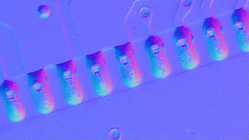
Surface Normal: each pad appears as its own rounded mound.
FORESIGHT STEREO first estimates the surface normal, the direction the surface faces, at each pixel. Surface Normal encodes that direction as color. The same pads now appear one by one as rounded mounds: one side pink, the other light blue, because the slopes face opposite ways. The flat board surface is an even blue-violet.
Step 2: relief only (3D Surface)
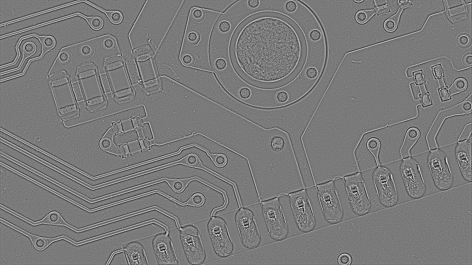
3D Surface: traces under the solder mask, component steps, and via rings stand out as relief.
3D Surface drops color and renders only the surface relief. Across the full field of view, traces under the solder mask, barely visible in Live, become distinct raised lines. The outlines of the pad row, the steps of the chip components, and the rings of vias also read clearly in relief.
Step 3: the 3D view
Back to the image at the top. Built from those surface normals and shown at an oblique angle in FORESIGHT STEREO Viewer:
- Solder pads line up as rounded mounds, with fine surface texture visible in 3D.
- Chip components rise from the board like boxes, and the step at the electrode ends is visible.
- Traces run under the solder mask as low ridges.
- Vias appear as small dimples and rings; the inside of the large hole appears as a rough surface.
How one capture becomes a 3D shape
With the camera and board held fixed, TR-100 captures eight images while switching between eight lighting directions. The brightness of each point changes with the lighting direction, and comparing those changes gives the surface normal at every pixel. Integrating the slopes derived from the normals then reconstructs the surface shape.
FORESIGHT STEREO is our own development of this principle, known as photometric stereo. Learn more on our 3D reconstruction page.
One caveat: the 3D view is for seeing shape, not for reading off real dimensions. Integration does not directly give absolute height, and the view may exaggerate the vertical axis for visibility.
Where this could help in PCB inspection
This was a good board, so nothing here is a finding about faults. Still, a view like this may be useful when considering inspection items where shape matters, such as:
- Solder volume and shape (fillets, insufficient or excess solder)
- Lifted or tilted components
- Foreign material
- Dents
These are general examples; none of them were observed in these images.
Next steps
Under the glare in a photo, there are solder mounds, component steps, and trace ridges, and TR-100 shows them in 3D from a single capture. Evaluating boards with real assembly faults is the next step.
Want to see the shape of your own boards? Contact us to arrange a test capture, or learn more about TR-100.
